|
|
EBSD and BKD |
|
|
|
Basics of Electron Backscattering Diffraction in the SEM
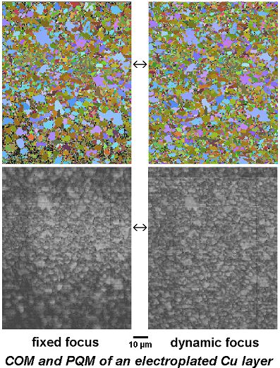
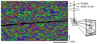
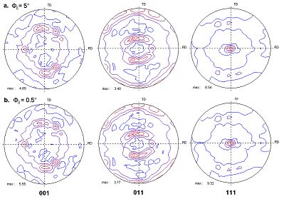
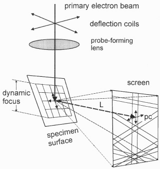
1. Pattern Formation Backscatter Kikuchi patterns (BKP), also known as Electron BackScattering Patterns (EBSD) are produced by incoherent wide-angle scattering of a stationary beam of high-energy electrons from a virtually perfect volume of crystal. A small fraction of these electrons are channeled along low-index lattice planes, leave the crystal and form a Backscatter Kikuchi pattern on a phosphor screen placed close to the specimen. It consists of straight Kikuchi bands whose widths are, according to the channeling conditions, proportional to the Bragg's angles. The center lines of the bands correspond to the (imaginary) section lines of the lattice planes with the screen, the star-like band crossings to zone axes of the crystal lattice, and the angles between the bands to interplanar angles. Therefore, the crystal orientation of the grain under the beam can be determined with high accuracy by simply measuring the widths and the positions of several bands in a pattern. In the SEM, the patterns are recorded with a low-light level CCD camera, digitized, corrected for background and transmitted to a PC for indexing. 2. An advanced BKD System Texture analysis and characterization of microstructure require a large number of grain orientations to be measured on a selected area on the specimen without the interaction of the operator (Automated Crystal Orientation Measurement/Microscopy = ACOM, or in short Orientation Microscopy (OM)). For indexing a pattern and determining the grain orientation, the positions of at least three bands in the pattern are required. The band positions are extracted automatically by applying a Radon or Hough transform (see below). In advanced EBSD systems, preference is given to digital beam scan, due to higher speed and precision, over a mechanical stage scan [1]. To make allowance for the strong forward scattering of fast electrons and to obtain sufficiently intense patterns, the specimen is steeply inclined to make a shallow angle of typically 20° with the primary beam. The specimen tilt, however, has an unwanted side effect on systems with digital beam scan in that the diffraction geometry changes from one measured point to the next and that the beam spot runs out of focus when scanning down the specimen one line after the other. Therefore, the specimen-to-screen distance and the pattern center have to be calibrated automatically from point to point, as well as the probe-forming lens has to be focused dynamically. The microscope is under full control of the ACOM program during automated measurement. When automated calibration is implemented in the EBSD system, the operator need not bother about keeping a fixed working distance. The band geometry is extracted on-line in a fast pattern recognition subroutine by applying a Radon transform. The higher the diffracting crystal volume is plastically deformed, the more diffuse the Kikuchi pattern appears to be. Pattern quality, as a measure of local plastic deformation, is hence determined by applying a 1D FFT on the Radon transformed pattern and by weighting the high spatial frequencies of the Radon peaks of the most prominent bands. Performance Spatial resolution is better than a tenth of a micron, depending on the spot size of the beam, the accelerating voltage and the density of the material. Resolution does in principle not depend neither on the beam current nor on the actual microscope magnification. The specimen area accessible to OM measurement is thus only limited by the lowest microscope magnification provided that the beam is focused dynamically. Since some EBSD systems are equipped with a camera of poor sensitivity, the spot size of the SEM has then to be widened unduly in order to obtain sufficient beam current, and hence spatial resolution gets worse. Depth of information beneath the surface is in the range of the mean free path of the backscattered electrons (estimated at some 10 nm only). BKD is thus a surface sensitive method. Special care is required in preparing clean specimen surfaces free from artifacts. The accuracy of grain orientation measurement is < 0.5°. A test of spatial resolution and accuracy can be performed by mapping a specimen that contains fine deformation twins. Dynamic system calibration can be checked by scanning across a large single crystal (e.g. silicon) at low SEM magnification and verifying the uniformity of orientation data. Speed of advanced BKD systems exceeds several hundred thousand measured orientations per hour. Typical shortcomings of previous EBSD systems are: Neither automated system calibration nor pattern calibration "on-the-fly" is available. Dynamic focusing is not provided, or the standard dynamic focusing appliance of the SEM is employed. Due to the steep specimen tilt and the high sensitivity of the quality of BKD on spot size, precise focusing is essential not only at low magnifications, but also for studying fine grain materials. The requirements for dynamic focusing are alleviated to some extend in the SEM with a field-emission gun due to the much smaller beam aperture and hence the larger depth of focus as compared to older SEM with a tungsten gun. Camera sensitivity is insufficient. Indexing is performed by only considering the center lines of Kikuchi bands rather than the center lines and the band widths, i.e. the interplanar angles and the Bragg angles Indexing is done with only a few bands since the Hough transform and the band tracing algorithm are inadequate to provide a sufficient number of located bands (N.B.: Typically 7 or more located bands should be available for cubic symmetry, and about 10 bands or more are desirable for lower symmetries.) Dynamic focusing in an advanced BKD system
3. Calibration of specimen tilt, pattern center and camera length
Caution: The surface of silicon wafers is usually inclined by several 0.1° to [001]. Check for this inaccuracy by rotating the standard specimen about its normal and eliminate the deviation. Provision has to be made that the x direction in the specimen surface is perfectly parallel with the x direction, i.e. the lines, of the scanning field. Otherwise a rectangular scanning field is heavily distorted, due to the steep specimen tilt, to a trapezoid. The y loci on the specimen differ from the supposed positions of a horizontal line by a factor of about (sin ε ⋅ tan 70°) whereby ε is the angle of deviation. Hence a static system calibration as well as the focus may not be correct. In this case the orientation data are not correct as well, unless the specimen is rotated by -ε around the optical axis of the SEM. Modern SEM provide a scan rotation unit to align the scanning directions interactively. If the focus is corrected dynamically across large scanned areas at low magnifications, the scanning field is usually rotating as well with increasing field strength of the probe forming lens. Dynamic calibration can correct the orientation data for small misalignments ε of the scanning field with respect to the x axis of the specimen. Interactive calibration methods The specimen-to-screen distance enters calculation as a magnification factor. If solely the center lines of the bands, i.e. the interplanar angles, are used for indexing, the specimen-to-screen distance is skipped together with the lattice constants in the case of cubic crystal symmetry and hence is not required. However, it is strongly recommended to make use of the Bragg angles, i.e. the band widths, as an additional information to increase the reliability and accuracy of indexing. In this case, and for non-cubic crystals, the specimen-to-screen distance and accelerating voltage must be know as well. The pattern center is defined as the footpoint from the actual position of the beam spot on the tilted sample surface to the phosphor screen. It represents the center of gnomonic projection of the pattern. It is crucial for correct indexing of the bands and determination of the reference sample directions to know the pattern center with high accuracy. An experienced operator can roughly locate the pattern center by visual inspection and by trial-and-error until indexing is performed successfully. Several interactive calibration methods enable the pattern center to be recognized without having to index a pattern [3-5]: Automated calibration methods The full information about the geometry of the setup is in principle contained in a single pattern already. The pattern must provide at least seven clear bands, either by interactive or by automated band detection. A smart scan of much of the calibration space is then performed, considering the effects of gnomonic projection on the widths and positions of the bands, for searching the best possible calibration parameters. For cubic crystals only the lattice symmetry (fcc, bcc, diamond lattice) and a good estimate of the accelerating voltage must be known. Crystals of lower symmetry, however, require the knowledge of the lattice parameters. The calculation will usually take less than one minute and provides very good approximations of the pattern center and the specimen-to-screen distance [1]. This method is called "Automated Setup Calibration". If indexing of a pattern has already been performed successfully and thus the crystal orientation is known, the accurate position of the pattern center as well as the camera length are obtained from a least square fit of the simulated band positions to the measured bands [2]. In most cases about five or six bands, equally distributed around the center, are sufficient [1]. As for the automated setup calibration, the symmetry of the cubic lattice (fcc, bcc or diamond), respectively the lattice constants, and the accelerating voltage must be known. The method is called "Automated Pattern Fitting Calibration". It is usually following automated setup calibration as a refiner. A precise system calibration is thus conveniently performed within an instant. In an advanced EBSD system, automated setup calibration followed by automated pattern fitting calibration is carried out - always before the acquisition of an orientation map is started - in or very close to the four corner points or at least at the start and end point (two points) of the scanning field. The microscope has to be focused, under visual control by the operator, for best pattern quality in the four respectively two corner points of the scanning field. The calibration parameters are stored together with the focus settings (i.e. the working distances or objective lens currents) in the setup file. They have to be adjusted "on the fly" for every scanned point on the sample: When the beam is scanning down across the tilted sample surface, the x and y coordinates of the point of beam impingement as well as the working distance, the camera length and the pattern center vary. The actual values of the pattern center and the specimen-to-screen distance are readily calculated by interpolation of the calibration data in the corner points of the scanning field. They are used in the indexing routine. This procedure is called "Autocalibration " [1]. For very low magnifications there may be still a slight deviation from the accurate values. As a program option, automated pattern matching calibration can be applied to every indexed pattern for fine tuning. Orientation calculation is then repeated with these refined parameters. They are also used as initial values for the subsequent pattern of the scan loop. If autocalibration is not carried out, errors in calculated grain orientations may exceed several degrees or indexing may fail, in particular at low magnifications. A simple test on the accuracy of automated system calibration can be made by measuring across a large field on a single crystal and checking the uniformity of orientation data. The current through the objective lens, i.e. the focus setting, has to be adjusted from one to the next scan line. The actual value is calculated by interpolation between the stored focus settings in the corner points of the scanning field, and adjusted automatically by the computer of the advanced EBSD system through the computer interface ("Dynamic Focusing") [1]. Missing correct focusing may cause wrong orientation data or failed indexing, in particular at low magnifications and fine grains. The built-in dynamic focusing facilities of most SEM do not support the high sample tilt of the EBSD setup. Therefore, the focus of SEM has to be controlled by the BKD program, not only the beam deflection.
An automated BKD system using mechanical stage scan with a stationary primary beam rather than digital beam scan does not need a sophisticated calibration technique nor dynamic focusing, since the diffraction geometry, i.e. the pattern center and the specimen-to-screen distance, stays constant during crystal orientation mapping. The sample has only to be placed in at that working distance for which the system has been calibrated beforehand
by performing
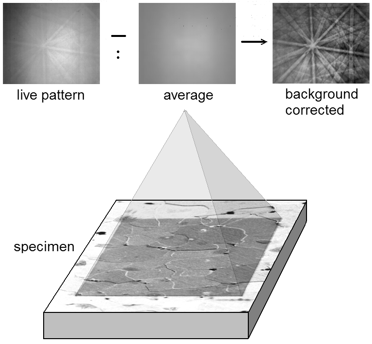
one of the cumbersome interactive calibration methods. These systems are usually set-up calibrated with a single crystal and finally calibrated with the moving screen method for several working distances. The calibration parameters are then stored in a look-up table, and the actual working distance is directly displayed on the SEM panel after focusing, or checked for from reading the objective lens current. 4. Background correction The useful image signal makes only a few percent of the Backscatter Kikuchi Pattern. Therefore, the uneven strong background has to be removed. This is usually done be subtracting a flat background image or by normalizing (i.e. dividing pixel by pixel) the pattern on a flat background image. Flat background images can be obtained in several ways: 1. Static integral flat fielding is performed either by extremely defocusing the primary beam, or by scanning over a large area and integrating the patterns so that the structures of the Kikuchi bands are equalized. The beam spot can either be positioned at random on the whole scanned field, or at some sections of the field.
With conventional EBSD systems the flat fielding background image is acquired at the outset of the session in the SEM and readily applied to every acquired pattern. With the Fast EBSD system the integral background image my be stored along with the pattern sequence on the hard disk, or it is constructed later-on out of some sequence patterns before off-line indexing. Static integral flat fielding suffers from several disadvantages: The background gradient is moving with the beam spot position on the specimen, in particular at large scanned fields. Background depends on beam current fluctuations and variations in detector sensitivity and surface relief. Background strength and gradient vary with the actual grain orientation as well as the density and the surface state of the material which is significant when studying multiphase materials. 2. Dynamic local flat fielding of each pattern on its individual background is superior to applying the same global integral flat background image on all patterns. The background image for dynamic local flat fielding is obtained by binning down the pattern to about 1/10th or less of its size, refining it again to the initial size and finally applying averaging filters. Dynamic local flat fielding has been the default technique for background correction in Fast EBSD. 5. From the raw backscatter Kikuchi pattern to the Radon transform
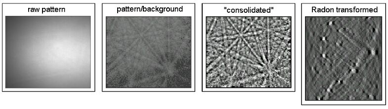
It is common practice to use backscatter Kikuchi patterns with a digitization depth of 256 gray levels. Background is removed. The raw patterns are reduced in resolution, for the sake of speed, to typically 100x100 pixels (consolidation). In the subsequent processing procedure, noise is further reduced and contrast enhanced by applying non-linear operators in Radon space [8]. ______________ |
||||||||||

 The grain orientation is calculated from the Kikuchi pattern projected on the phosphor screen. Therefore, the orientation of the coordinate system which is fixed to the screen has to be exactly known with respect to the reference coordinate system fixed to the specimen. In particular the x direction in the specimen surface
has to be perfectly
aligned parallel with the phosphor screen and the specimen tilt must be known. The correct position of the specimen surface needs to be checked before any other measurement can be carried out.
The grain orientation is calculated from the Kikuchi pattern projected on the phosphor screen. Therefore, the orientation of the coordinate system which is fixed to the screen has to be exactly known with respect to the reference coordinate system fixed to the specimen. In particular the x direction in the specimen surface
has to be perfectly
aligned parallel with the phosphor screen and the specimen tilt must be known. The correct position of the specimen surface needs to be checked before any other measurement can be carried out.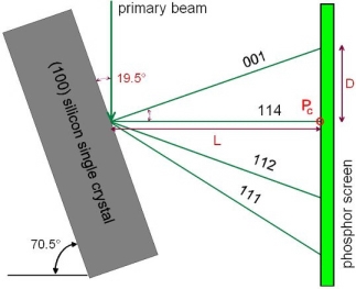 The angle of specimen tilt and its rotation around the optical axis (direction of the non-deflected primary beam, z axis) is usually calibrated by using a <100> silicon crystal as a standard reference specimen [3]. For a tilt angle of 70°30' out of the horizontal to the primary beam direction, the <114> pole falls on the pattern center in a direction normal to the optic axis, and for a tilt angle of 35°16' the <112> pole direction is normal to the primary
beam.
Hence the actual specimen tilt can readily be obtained from the spacing between the pattern center and the <114> or the <112> pole, respectively.
The angle of specimen tilt and its rotation around the optical axis (direction of the non-deflected primary beam, z axis) is usually calibrated by using a <100> silicon crystal as a standard reference specimen [3]. For a tilt angle of 70°30' out of the horizontal to the primary beam direction, the <114> pole falls on the pattern center in a direction normal to the optic axis, and for a tilt angle of 35°16' the <112> pole direction is normal to the primary
beam.
Hence the actual specimen tilt can readily be obtained from the spacing between the pattern center and the <114> or the <112> pole, respectively.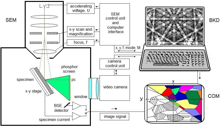
|
|