|
|
EBSD and BKD |
|
The evaluation of
grain orientation data 1. Indexing of Kikuchi patterns The characteristics of Kikuchi patterns are bands that are regularly arranged on a continuous background. They are delimited by straight lines. Strictly speaking, the edges of the Kikuchi bands are hyperbolas formed by the intersection of the Kossel cones with the plane of the detector. The intensity distribution in a Kikuchi pattern is not explained by a simple geometric model, but the dynamic theory of electron diffraction has to be employed [1]. The mechanisms that lead to the formation of the characteristic diffraction features in EBSD patterns, including Kikuchi bands as well as prominent circular Kikuchi envelops around zone axes (by appearance like HOLZ lines from thin foils in CBED), have been explained, and excellent agreement has been obtained recently between experimental patterns and simulations in extended many-beam dynamical calculations using the Bloch wave approach [2].
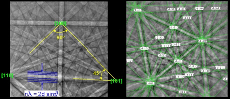
For indexing it is sufficient to consider a pattern as a gnomonic projection of the crystalline lattice of the known phase on a plane detector. The point of impact of the stationary primary beam on the surface of the sample, or more precisely the volume of interaction in the grain, is the center of the projection. We can imagine that the planes of the lattice are stretched out until they cut the center lines of the associated Kikuchi bands. So, the angles between the center lines correspond to the interplanar angles. The "stars" at the crossings of the bands correspond to the axes of the crystal zones (see pattern on the left). The angular width of a band is equal to twice the Bragg angle ϑhkl :
is a good approximation of the de Broglie wavelength of electrons at low to medium energy. A relativistic correction is necessary for accelerating voltages of about 100 kV and higher:
Exercise: Derive the rule of thumb
for the wavelength of a free electron after passing through an acceleration
voltage U from the De Broglie relation. The convergence of the primary beam is not relevant. The extinction rules due to the structure factor of the crystal lattice apply for expected reflections (i.e. Kikuchi bands), and high order reflections may appear as a set of straight lines parallel to the band edges. The center line corresponds to the trace of the plane of the Bragg diffraction and thus seems to be strictly fixed to the lattice. This is, in addition to the sharpness of the lines, the basis of the high precision with which the orientation of a crystal can be determined. The location of the Kikuchi lines, some of which are fractional, is difficult. They are extracted from the pattern by automated pattern recognition (see Radon transform). The localization of straight lines can thus be reduced to the search for isolated peaks in Radon space which stand for Kikuchi bands respectively Kikuchi lines. Indexing is accomplished after provision of the positions of 5 to 10 narrowest and most intense bands of two or more zone axes of a pattern. The geometry of the pattern is compared with the positions of the lattice planes in the elementary cell. The calculation is carried out in computer programs that use look-up tables of the diffraction pattern families (tables of reflectors, interplanar angles and diffracted intensities) for the considered lattice system.
With a multiphase material, the program tries to index the pattern with all the assumed crystal lattices. It accepts as true the solution and phase (phase discrimination) for which the backward calculated pattern (theoretical) best matches the measured pattern. Rough values for the geometric parameters (e.g. the position of the projection center = pattern center PC, the sample to screen distance = camera length L) are needed at the beginning. They are refined by a least square fit between the actual and
recalculated pattern. The crystallographic orientation of the grain is described either in (hkl)[uvw] notation, by three Euler angles (φ1, Φ, φ2), or by the rotation matrix g, which transforms the reference coordinate system of the considered sample into a coordinate system related to the crystal axes. Finally, by simulating the pattern, it is verified that the grain orientation and the chosen crystal structure
best fit the pattern. This check can also be illustrated by superposing the
theoretical pattern on the experimental one (see pattern above on the right). The angular solution is limited by the precision with which the bands respectively lines can be localized in the pattern. Details of the indexing routine can be found for example in [3, 4]. Several commercial EBSD systems are available on the market. 2. Pattern Quality PQ - an indication of the imperfection of the lattice
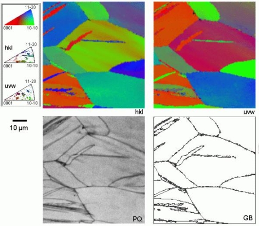
[1] J. Sukkau and R.A. Schwarzer: Reconstruction of Kikuchi patterns by intensity-enhanced Radon transformation. Pattern Recognition Letters 33 (2012) 739–743. 3. Orientation Microscopy The prime objective of orientation microscopy is the acquisition of grain orientation data. They are usually represented by three Euler angles or by the rotation matrix which rotate the coordinate system of the specimen in the coordinate system fixed to the particular crystal lattice. A clear graphical representation of the microstructure is obtained by constructing Crystal Orientation Maps (COM), or in short Orientation Maps (OM) [1]. Hereby the orientation parameters in the measured grid points are assigned in an image to unique shades of three basic colors that are red, green and blue. Orientation parameters in crystal orientation maps may be two crystallographic directions (hkl)[uvw] for two sample reference directions ("Miller maps"), the Euler angles (φ1, Φ, φ2) ("Euler maps"), or the Rodrigues vector R ("Rodrigues maps"). Finally an orientation map of the sample is obtained which illustrates the morphology of microstructure and the spatial orientation distribution of the grains. If abutting points in a region have the same or similar orientations as their neighbors, they are identified as a grain, and the intersections of such regions are called grain respectively phase boundaries. Grains with an orientation closely in common are represented by similar colors. It is so possible to quantitatively represent the orientations and misorientations in materials on the sub-micron scale. The misorientations between neighboring raster points are calculated and, by assuming specified threshold values, grain boundaries (GB) as well as phase boundaries can be marked out in the COM. However, a grain boundary in a planar sample section forms a closed perimeter line which must not "leak". A special "path finding" algorithm along the grain boundary segments is applied to fill missing spots where indexing may have locally failed, and a (binary) grain boundary network of the microstructure is obtained. The lines may be further skeletonized to one pixel in width. Grain boundaries are commonly marked by the Rodrigues vector, R, the axis-angle parameters of the misorientation, Δg, or the Σ character according to the CSL model. Other local properties or parameters can be represented graphically by color maps of the microstructure in a similar way, such as dislocation density, the predominant glide systems or twin systems in the grains, the Schmid factor or the residual deformation energy in the individual grains [2]. The advantages of grain-boundary COM over conventional light microscopical images of grain boundary networks are for stereological evaluation: Therefore, standard methods of quantitative metallography can directly be applied to skeletonized grain-boundary COM. In many labs sophisticated stereological programs are already available. 2D microstructure parameters can so be determined such as the area fraction, planar size, average grain size, shape and arrangement of grains, and their statistical distributions. If the phases in the material have sufficiently different lattice constants or differ in their element composition so that the phases can be differentiated - with the aid of simultaneous EDS analysis - in every pixel, quantitative metallography can be extended to a phase discriminating stereology. Under usual stereological assumptions, 2D stereology is often extended to 3D stereology to calculate such parameters as volume fraction, average grain volume, 3D shape and arrangement, contiguity of phases, and their statistical distributions. Approaches are made to reveal the true 3D microstructure on a grain specific scale by combining BKD with in-situ serial sectioning in a FIB&SEM instrument. Since a grain in the grain-boundary COM is represented by the group of pixels with similar grain orientations within the GB loop, its area fraction is simply measured by counting the raster points which are enclosed by the grain boundary perimeter line. This point-counting method is superior over the line-intercept method because it is not affected by concave sections of the grain boundary line nor by "islands" formed by a second grain underneath which may shine through the sample surface. A rapid but less precise alternative for estimating size and shape of grains is the visual comparison of a grain-boundary COM with standard grain charts or reticules.
The unique colors, on the other hand, can be interpreted in terms of orientation parameters by comparison with a color legend. The full grain orientation may be reconstructed from a set of two colored Miller maps in the following way: From the symmetrically equivalent orientations only those have been used for imaging whose Miller indices (hkl) of the in-surface planes fall in the standard triangle 001-011-111. One of the permutations of the Miller indices, [uvw], of an orthogonal direction is given in the standard triangle 001-011-111. For a full description of crystal orientation the sign and sequence of the Miller indices [uvw] is determined considering the condition of orthogonality between (hkl) and [uvw]. If this condition is fulfilled for more than one of the permutations of <uvw>, these solutions are symmetrically equivalent. They cannot be discriminated physically from each other, because the choice of the position of the axes of the elementary lattice cell is arbitrary. It is worth noting that conventional light or scanning electron microscopy images may display abutting grains by the same color or gray shade. Therefore, Quantitative Metallography may fail when deriving grain size distributions or other statistical parameters from microscopy images. In crystal orientation maps, however, grains (and phases) are discriminated unambiguously by indicating their crystal orientation and lattice structure. Since crystal orientation
maps are available in digital form by their way of construction, the derivation of statistical parameters (such as the distributions of grain size, length of grain boundaries, grain size as a function of grain orientation, and the fractions of Σ grain boundaries) is simply reduced to pixel counting. 4. Pole Figures and ODF The Orientation Density Function (ODF) and pole figures can be constructed directly from a data set of individual grain orientations by associating the orientations or the volume fractions of grains having these orientations with points or discrete cells of finite size in the Euler orientation space, on pole figures (stereographic projection) or on inverse pole figures (standard triangle of the crystal symmetry group). With increasing number of data points such discrete representations are difficult to survey. So they are often normalized, smoothed, filtered and converted to equal density line representations, or the densities are scaled to color intervals in the plots of ODF sections, pole figures or inverse pole figures. This method of discrete representation appears easy and straightforward, but has drawbacks even if the Euler plots and Pole Figure Plots are smoothed and normalized to equal densities. First, the distortions of the Euler space for small Φ angles are usually not taken into account (nor the distortions of the stereographic projection) since for simplicity the Euler space is subdivided into cells of constant angular increments. Second, the number of measured orientations is often not high enough to guarantee statistical relevance. An elegant approach to smooth and to condense the data set into a continuous representation is the calculation of the ODF, f(g), by series expansion into generalized spherical harmonics (T functions) after Bunge [1]: The expansion coefficients (termed "C coefficients") are then expressed by Vs stands for the volume fraction of grain s, and Ks(l) for the convolution kernel of the expansion. Common convolution kernels are a Dirac δ function in case of a large number S of orientations, or Gauss type distributions in Euler space with a half width Ψ0s at 1/e maximum of the Gauss peak at the orientation point gs [2, 3] The C coefficients are a highly concise and convenient description of crystal texture. They enable the calculation of normal and inverse pole figures, important elastic and plastic materials properties, and tensorial properties in general [1]. ODFs calculated from EBSD and from X-ray pole figure measurements usually agree very well if the data have been acquired on the same specimen area. N.B.: In X-ray diffraction, the reflections and hence pole figures are indexed according to their diffracting lattice planes {hkl}. By tradition, inverse pole figures referred to the specimen surface are also indexed according to the in-surface lattice planes rather than to the crystallographic directions perpendicular to the specimen surface. This inconsequent definition is of no relevance in case of cubic crystal symmetry, but has to be kept in mind
when studying
materials of lower symmetry.
You should keep in mind: 5. The Microstructure Function The meso- and microstructure of a polycrystal is described by the distributions of size, shape, arrangement, orientation and defects of its constituent grains and phases in three-dimensional space. A mathematical quantification of this state is given by the Microstructure Function G [1] (also named Aggregate Function) [2, 3]: The phases i, the crystal orientations g and the lattice defects D in the volume elements are specified at the places r = {x, y, z} in the specimen. g = {φ1, Φ, φ2} are the orientation parameters, D = {d1, d2, ..., dn} the substructure parameters, and i = { i1, i2, ..., in} the phases which are characterized by their crystal lattice and element composition. In the simplest case, that is a single-phase material without considering the grain substructure, the microstructure function G(r) still depends on six coordinates that are the three spatial and the three orientation parameters. They make up a six-dimensional space which is almost beyond human imagination. So a split was made in traditional materials science by either emphasizing the morphology of microstructure or the density of grain orientations. Two
branches of science have developed almost without mutual interaction: It is a unique feature of orientation microscopy in the SEM that this technique enables the acquisition of the microstructure function at a high spatial resolution with reasonably low effort: Scanning across the specimen surface in a raster grid yields two spatial coordinates {x, y} of the measured location. The third dimensional coordinate {z} can be obtained in principle by serial sectioning. The grain orientation, g, is the prime objective of orientation microscopy and readily available along with {x, y}. Phases are described by their crystal lattice. Additional information about the local element composition, e.g., from a simultaneous EDS analysis, may be helpful in phase discrimination to rule out less likely phases before performing the lattice check. Pattern quality is a (qualitative) measure of local dislocation density and lattice strain. To enable a comprehensive orientation-stereological interpretation of the microstructure, pattern quality, confidence index, and the concentrations of several elements (if measured simultaneously by EDS) are stored along with the grain orientation data for every point (x, y). With the availability of automated EBSD the route is now open to a comprehensive "Orientation Stereology" by merging both aspects of microstructure [1]. Depending on the application under consideration, several special functions may be derived from the universal microstructure function G(r) which are either sections through the six-dimensional space or integrals of it. Texture descriptors are the Orientation Density Function (ODF), f(g), pole figures, the MisOrientation Distribution Function (MODF), orientation correlation functions, and texture fields. Of particular interest for applications in industry
are
tensorial
materials properties that can be calculated from orientation data if the anisotropy of the property is known for the single crystalline material [4]. 6. Electromigration failures in copper interconnect lines
In the crystal orientation maps the grains are clearly discriminated from each other. Some twin grains are seen. It is worth mentioning that individual grains are hardly recognized in conventional SEM micrographs, since orientation contrast with backscatter and secondary electrons is low. A fragmented central seam of grain boundaries has formed. The ODF and pole figures have been calculated with the series expansion method from the measured crystal orientations, separately for those grains which fill an interconnect line at full width ("bamboo grains") and for those grains which form the central seam. For both types of grain, a strong <111> and a weak <115> fiber texture have been found. For the bamboo grains, the fiber axes are aligned in specimen normal direction, i.e.
from the bottom to the top of the trenches, whereas for the seam-forming grains the fiber axes are directed perpendicular to the sidewalls. 7. Gentle sample preparation of metals and ceramics for EBSD The first requirement for electron microscopy is to have samples that are stable in a vacuum and under the impact of high-energy electrons. They must possess a minimum of electrical conductivity so as not to become charged [1]. The usual surface coating with a layer of sputtered gold, as in conventional imaging, is contraindicated for EBSD due to the shallow interaction depth of primary and diffracted electrons. Extremely thin carbon films on a grid-like support can serve as grounded conductors. Electric charge can be avoided in a variable-pressure SEM with moderate vacuum down to a few pascals, or with a gas jet in the sample chamber. SEM EBSD is performed on solid samples. The main requirements are a flat, clean surface, free from preparation artifacts such as accidental deformation, reaction layers or phase-selective etching. Electro-chemical mechanical polishing (ECMP) [2] is often a good choice for metal samples, in particular if supported by placing the sample at positive potential of some 10 V during mechanical polishing with a suitable electrolyte. A finish by ion polishing (e.g. Ar+ at about 1 keV and flat angle of incidence) may be advisable to remove residues and oxide layers from the preparation steps. Ga from a FIBing treatment, however, tend to segregate at grain boundaries in Al and Mg samples. At present, EBSD is mainly used for metal samples. Non-conductors, ceramics and sensitive samples require special treatment. They are often brittle or decompose under the electron beam. The preparation of a clean and flat surface is crucial: charging and cathodoluminescence (which can interfere with the electron detector) are a challenge. Parasitic magnetic fields and surface contamination, i.e. an unwanted surface layer due to hydrocarbons from polymerized residual gas in the sample chamber, are problematic. Foreign layers weaken and obscure the diffraction patterns, while deformation layers broaden the Kikuchi bands, resulting in diffuse patterns. All this has a negative effect on the accuracy of the indexing. It is far less tedious to prepare a suitable bulk sample for EBSD than a thin electron-transparent film for TKD. In any case, sample preparation is the most important factor in optimizing performance. __________
|
|||||



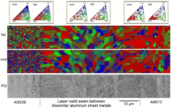
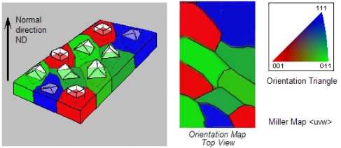 For orientation maps using Miller indices as orientation parameters, a color triangle is overlaid on the stereographic standard triangle of the crystal lattice under consideration [1]. In case of cubic crystal symmetry red is commonly assigned to directions near the (001) corner, green to directions near the (011),
and blue to the directions near the (111) corner. Using this legend, colored Miller maps provide an illuminating display of the spatial and angular distribution of crystallographic directions related to reference directions in the sample, for instance the sheet normal direction, ND, and the rolling direction, RD, in rolled sheets. Two Miller maps are required, one for the {hkl} in-surface planes (i.e., in case of cubic symmetry the <hkl> directions perpendicular on the specimen surface), and one for
the <uvw> in a reference direction in the specimen surface, to fully represent the grain orientations in the surface. When both Miller
maps are considered, the spatial and angular distribution of crystallographic orientations is clearly visualized.


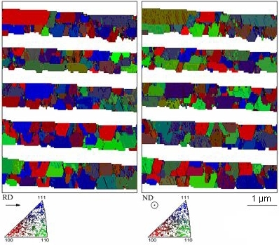 About 1 μm thick copper layers have been electroplated on trench-structured SiO2 /Si substrates by the damascene technique. The trenches were 1.0 μm wide, 0.5 μm deep and PVD coated with 50 nm Ta as a barrier layer to protect the silicon semiconductor from diffused
copper.
In addition, a PVD copper seed layer has been deposited at 50 °C. After the electroplating process the wafers were annealed for 10 min. at 120 °C. Finally the continuous copper layer has been removed by chemical-mechanical polishing (CMP) down to the damascene trenches to achieve narrow interconnect lines with sharp edges.