|
|
EBSD and BKD |
|
|
|
Transmission Kikuchi Diffraction TKD The first Transmission [1] as well as Backscatter [2] Kikuchi Patterns (later named TKP resp. BKP) were published in the same volume of Proc. Imperial Academy of Japan (Tokyo) 4 (1928) pp. 271 ff. resp. pp. 475. In the TEM the diffraction patterns are either acquired with a camera placed on-axis at the bottom of the microscope column or with a retractable camera on the side-entry flange above the viewing screen. A circular continuous density filter in the optical path is of advantage to equalize the steep drop of intensity from the blooming primary beam spot to the dim marginal area. Pattern intensity is of minor concern in TKD with a TEM. The patterns should cover a large angular range and be undistorted. These requirements limit TKD orientation mapping to the use of a TEM with a condenser objective lens and microbeam diffraction facility such as for instance the Philips CM series, respectively FEI TEM. For automated mapping [3] a computer controlled scan of the beam spot has been implemented. For details and applications see http://www.crystaltexture.com/tkd.htm .
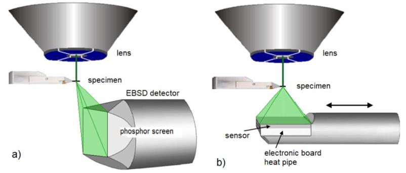
TKD setup in the SEM for indirect detection using a phosphor screen optically coupled to the camera sensor TKD in the SEM works with a thin sample that must be at least partially transparent to electrons. The foil is positioned horizontally in a special holder (see also section FastEBSD) [7]. Indirect detectionin the SEM uses a phosphor screen optically coupled to a sensor chip or a CCD or CMOS camera. In the conventional
setup (Fig. a), a standard EBSD detector is used, but it is mounted further down under the sample [4, 5]. The vertical phosphor screen covers about half of the backscatter cone and is imaged with an optically coupled, low-light CCD or CMOS camera. An alternative setup uses a special EBSD detector in which the transparent phosphor screen is located horizontally about 1 cm under the sample. A mirror at an angle of 45° on the back of the screen reflects the pattern onto the camera [6]. In a slim device, the phosphor screen may directly be placed on the CMOS sensor chip (Fig. b). A higher sensitivity is made possible and any optical distortions are avoided in this lens-free configuration. The advantage of these setups with a horizontal screen is that the entire cone of the Kikuchi pattern is captured, as in a TEM with a side-entry CCD camera. However, the intense central beam spot can overexpose the camera resp. sensor due to the limited dynamic range, while the edges of the pattern have too low an intensity for evaluation. A circular continuous density filter in the optical path is recommended, as with TKD in TEM. Directly pixelated detectors lead to a significant improvement in detective quantum efficiency (DQE) as the collected electrons are directly converted into intensity data [8]. The detector is mounted concentrically to the primary beam spot below the sample in a horizontal position (Fig. b). The phosphor screen is dispensable. A high speed of several thousand frames per sec. is possible [8]. Spatial resolution in EBSD and TKD A high spatial resolution in orientation measurement is required for the study of fine grain and heavily deformed materials in general, of recrystallization and grain growth, of grain boundary characterization, of nanomaterials and in the study of the impact effects of high-energy particles. But why does spatial resolution in Kikuchi diffraction fall more than one order of magnitude behind spatial resolution in conventional SEM imaging, and still further behind when compared to the spatial resolution of a TEM? The inherent resolution limit of Kikuchi diffraction is set primarily by the excitation volume rather than by the diameter of the beam spot at the point of impact on the sample surface. The excitation volume is the fraction of the interaction volume of the primaries with the sample from where the pattern forming electrons are diffracted and can leave the crystal with no further scattering. Gray shading in the figure indicates this volume fraction. The footprint of the beam spot is marked in bright green. A further limitation of spatial and depth resolution in Kikuchi diffraction is set by the smallest grain size. To exclude overlapping Kikuchi patterns, grain size should be larger than the excitation volume. Spatial resolution with copper is better than 0.05 μm at 20 kV using a tungsten filament and presently about 0.02 μm with a FE gun. The pattern is formed on the exit side of the foil in a depth of about the free mean path of the electrons. Patterns generated close to the entrance side are blurred due to inelastic scattering and thus contribute mainly to background. Therefore, a thin (amorphous) layer on the entrance side only widens the beam.
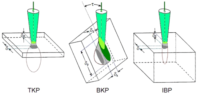
Resolution in depth, δz, simply equals foil thickness. In practical work, the smallest probe size and hence spatial resolution is limited to about 10 nm with TKD, due to the decrease in image brightness as the probe becomes smaller, and due to the spread of the scattered beam on its way through the specimen foil. If neighboring grains are studied, orientation differences down to 0.1° can bemeasured with TKD in the TEM and about 0.5° in the SEM. While resolution within a grain is of lower significance, it becomes quite critical when the beam spot approaches a grain boundary. A smart pattern indexing software can then improve resolution in TKD and EBSD by taking account of the intensity levels of superimposed patterns, rejecting less likely orientation solutions and comparing orientations in neighboring pixels. Resolution in depth, δz, simply equals foil thickness or is less. Pattern contrast strongly depends on foil thickness, density and accelerating voltage. A promising alternative to EBSD will be crystal orientation mapping using Ion Blocking Patterns (IBP) [9]. These patterns consist of a bright even background superposed by a regular system of very sharp black lines. An IBP is similar to quasi a negative image of a BKP. A black line is formed by ions which impinge on the surface parallel with a low-indexed lattice plane, channel deep into the crystal, but cannot leave the crystal unless they are backscattered again in the channel of an angular width of less than twice the Bragg angle to the lattice plane. As a consequence of the small deBroglie wavelength of ions the lines are significantly narrower than the corresponding bands in BKP. A thin foreign amorphous layer fans out the incoming beam by scattering, thus suppresses channeling into the crystal and lastly the formation of black lines. The requirements for a gentle sample preparation and a clean vacuum are very high. At present commercial ion scanning microscopes with high current densities in small probes in the nanometer range and a clean vacuum in the specimen chamber are not yet available. Spatial resolution equals the footprint of the ion probe on the surface. Foil thickness and buckling set limits to TKD Thin foils are often difficult to prepare from the bulk. It is in many cases questionable whether a thin foil truly represents the structure of the interior of the material. The grains relax on both surfaces when the matrix is removed. Due to different grain orientations in a polycrystal the foil contains local residual stress. Therefore surfaces of freestanding foils are often not really flat but show a grain-specific surface relief and bulging. This foil bending and puckering cannot be easily excluded. The result is a change in local orientations of up to some degrees with respect to the microscope-specific reference directions. A large grain or a single crystalline foil is bent, but roughly retains its intrinsic orientation. This is visualized in the grain orientation map by color shading for low deviations in orientation. At larger surface slopes, pattern indexing may jump to another solution, which is correct for the microscope-specific reference directions (x, y and z) deviating from the local grain-specific reference directions and the local surface normal, but is not correct for the orientation if it could have been measured in the bulk material. Such jumps in orientation are reproduced by distinct color skips in the orientation map. Irregular bending and wrinkles are readily perceived in orientation maps of single crystal foils at large area scans since the resulting damask pattern appears factitious. The tiling of fine grains in a wrinkled foil, however, follows the local bending. The superposition of the surface topography and the rotated orientations of the individual grains result in a distinct color, presumable without shading, for each grain in the orientation map. If texture is not extremely sharp the map looks like a map of a usual fine grain polycrystal. Foil wrinkling is thus disguised. The slopes of foil bending are in the range of several degrees. As a consequence measured local orientations scatter by an error of this range about the orientations one would obtain if the sample were flat. The ODF and pole figures are slurred by widening sharp peaks of orientation densities by several degrees as well. Ideal thin samples with bulging inclinations below the angular resolution of a Kikuchi system are very hard to realize. This is true in particular for transmission studies in the SEM where foil thickness has to be much smaller, to be transparent at the lower accelerating voltage, than in the TEM at medium to high accelerating voltages. Dedicated sample preparation techniques are absolutely essential. A compromise between correct measurement on a flat surface and a reduced spatial resolution is to deposit the specimen foil on an amorphous support film. The specimen is then placed upside down in the microscope. The amorphous support widens the incoming beam by scattering, but contributes merely to the background in the pattern. Foil buckling is nicely displayed in "bend contours", also named "extinct ion contours", in TEM micrographs [10]. They are formed preferably at lower magnifications when a small selector aperture is used. They are dark in bright field images, respectively light in dark field images, for crystal regions where the lattice planes are in Bragg position. Contours of equal intensity represent lines of equal inclination to the electron beam. The angular deviation between contour lines is thus a multiple of the Bragg angle. [see TEM textbooks for details, e.g. [11], Section 3.2.3.3 Bend contours; and [12], Chapter 23.4 Bend Contours (Annoying Artifact, Useful Tool, and Invaluable Insight] Synoptic Overview
__________ S. Kikuchi: Diffraction of cathode rays by mica. S. Kikuchi: Further study of the diffraction of cathode rays by mica. S. Kikuchi: Diffraction of cathode rays by mica. (Part III) S. Kikuchi: The diffraction of cathode rays by mica. (Part IV) The summarization of these four articles on TKD appeared at the end of the same year in: |
||||||||||||||||||||||||||||||||||||||||

|
|